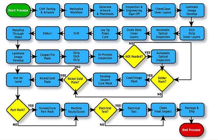
Getting rid of the unneeded copper step 5.
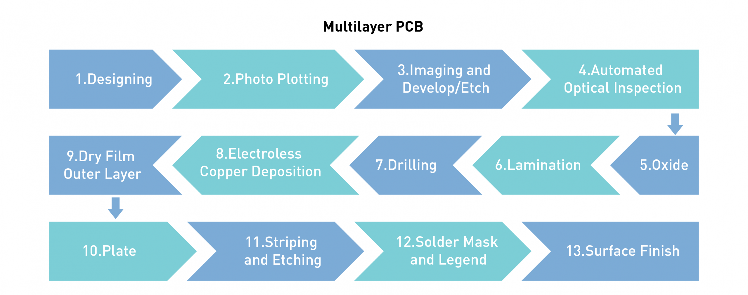
Multilayer pcb manufacturing process steps.
This is normally a three step process.
Because it is made by electronic printing it is called printed circuit board.
Electronic products in the production process there will be a printed circuit board production process.
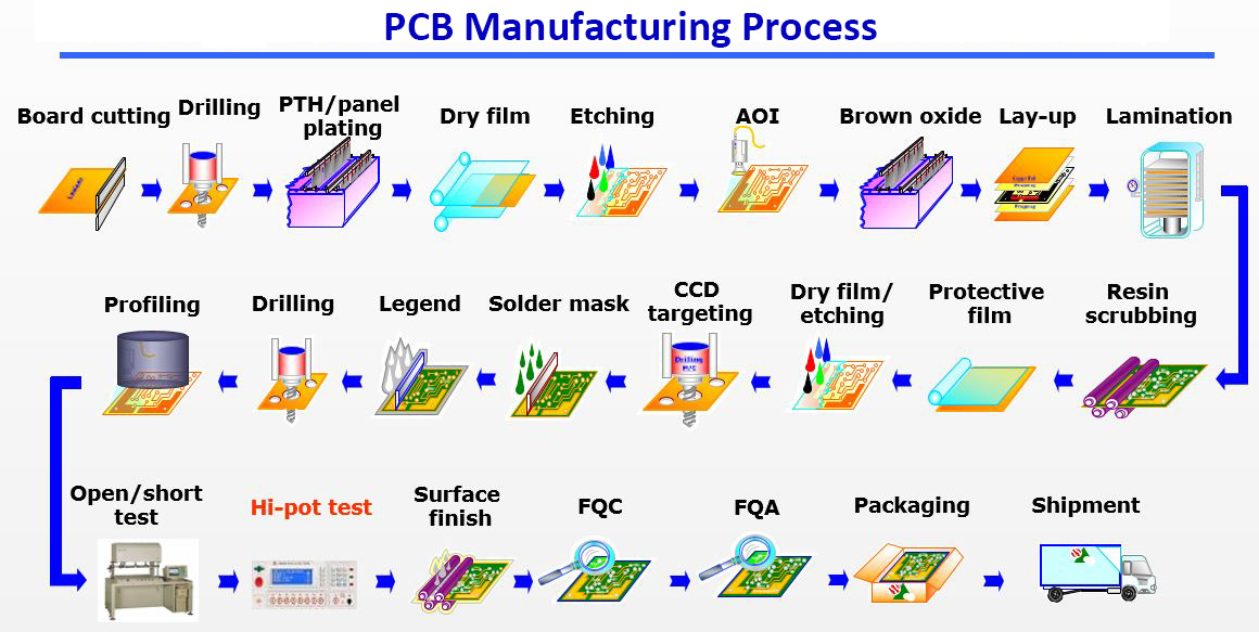
Finishing pcb and silkscreening step 15.
Soldermask for via holes pads.
Once we receive gerber data from the customer we send to cad department we check customer data meets our manufacturing requirements.
The second step is to etch away the exposed unwanted copper whilst the tin deposit acts an etch resist protecting the copper we need.
The last etching step 12.
Pcb plating step 9 10.
From raw materials to finished products everything is done right under the roof.
Gold plating for edge connectors.
The pcb goodness emerges victorious from within its shell of.
This is normally a three step process.
Soldermask on via holes with nickel gold finish.
A new soldermask for eurocircuits.
We check the track widths the space between tracks the pads around the holes the smallest.
Industrial pcb manufacturing steps.
Laminating the pcb layers step 7.
Imaging and plating the outer layer step 11.
Pcb manufacturing process steps step 1.
Direct imaging boosting the quality of pcb s.
Designing the pcb step 2.
With all the layers molded together in a super sandwich of pcb glory the technician simply unpacks the multi layer pcb product.
Electrical reliability testing step.
Printing the copper for the interior layers step 4.
Via holes in pads.
The third and final step is to chemically remove the tin deposit leaving the circuitry.
Drilling step 8.
Inspection and layer alignment step 6.
It s a simple matter of removing the restraining pins and discarding the top pressure plate.
These checks are mostly done automatically.
The process starts with designing layout of the pcb using any pcb designing software cad tool proteus eagle orcad.
Printing the pcb design step 3.
This process is like the one used to image the inner layers of a multi layer pcb.
This step in the manufacturing process begins by using a laminator machine to coat the outer layers of the bare copper panel with dry film a photo imageable material also known as photoresist or dry film resist.
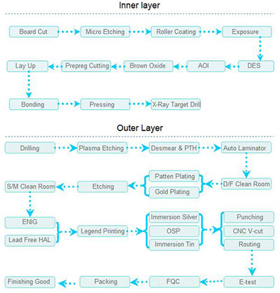
Making a double sided pcb.
Basic pcb manufacturing process step by step.
Pcb or printed circuit board is an important electronic part and the support body of electronic components.
The first step is to remove the blue dry film.
Which means they start from a and finishes with z of pcb manufacturing process.
Next step is to make the inner layer core.
The third and final step is to chemically remove the tin deposit leaving the circuitry.
Selecting the right surface finish.
Jlcpcb is a pcb manufacturing company with a full production cycle.
Applying the solder mask step 13 14.
Making a pcb step by step.